

The Context
Semiconductor wafer manufacturing needs stringent quality standards, so as to ensure optimum performance and efficiency of semiconductor devices. Moreover, processed wafers need to be free from any form of contamination. Plasma Cleaning Systems remove surface oxidation and clears mineral residue from wafer surfaces. Tismo was tasked with the development of an HMI for a state-of-the-art Plasma Cleaning System by one of the largest players in the plasma treatment systems market.
The Problem
The client’s plasma treatment product line was operated by control software, built on top of custom Graphical Widget/Controls. Tismo was entrusted with developing the HMI for the Plasma Cleaning System, using the client provided control library. The HMI would have to interact with a PLC server to control the overall operation of the system.
The Solution
Tismo developed the HMI for the Semiconductor Wafer Plasma Cleaning system, using C# and .NET. The factory design pattern was used for the HMI development. A common framework was used for similar screens, with the availability and visibility of certain controls changing according to each user type. All screens were designed such that they could be loaded into the main window and run in kiosk mode. Tismo was able to design an HMI that was compatible with multiple plasma cleaning systems. A button was provided in the HMI application to launch the UI according to the connected system.
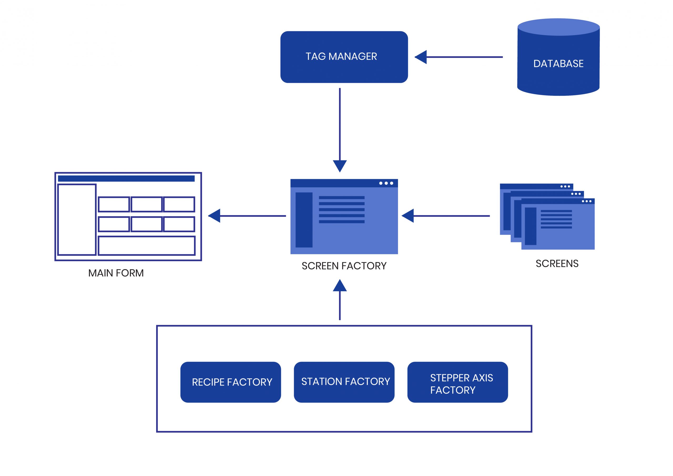
High Level context diagram of HMI for Plasma Cleaning System
Tismo used the client provided custom controls library and existing elements. The data from the PLC could be linked to the custom controls and manipulated using Tags. The Tags from the real-time database were also used to assign access controls to each functionality in the HMI. Access control could be initialized by the user through the application and the same access control object would be used throughout the HMI. A Dynamic Link Library (DLL) was referenced by the C# code for the HMI. Tismo designed HMI screens to support functionalities including production mode, which deals with the control for wafer processing lots, date and time settings, alarm history, various counters, status modes, maintenance modes, safety systems etc.
The HMI designed by Tismo was highly configurable and its universal architecture accommodated a multitude of handling configurations to support a wide assortment of wafer sizes and form factors. The HMI ensured tight controls over all process parameters, leading to repeatable results from wafer to wafer.
About the System
The Plasma Cleaning System developed by the client was highly configurable and resulted in high-throughput plasma processing and plasma cleaning for semiconductor and electronics packaging. The plasma chamber was capable of processes such as oxide removal, dielectric etch, organic contamination clean, photoresist descum/ash and surface activation. It supported manual and automated operations (with inline or built-in handler), SMEMA and SECS/GEM communications protocol, and remote user interface.
The chamber design allowed for interchangeable processing configurations and plasma modes – direct, RIE, downstream, and IFP (ion-free plasma) plasma treatment options. The system provided closed-loop plasma control that optimizes the RF system and minimizes tuning time. The system was designed to automatically compensate for changes in vacuum pressure, temperature and varied lot sizes.
Summary
Tismo developed an HMI for a Plasma Cleaning System used in Semiconductor Wafer Manufacturing. It was developed using C# and .NET, following the factory design pattern and utilized client provided custom Visual Basic (VB) libraries. The HMI was abstracted from the application logic and each control was registered with an existing library of variables, called Tags. The HMI was highly configurable, could accommodate various wafer sizes and form factors, was compatible with multiple plasma cleaning systems and supported numerous functionalities specific to semiconductor wafer handling.